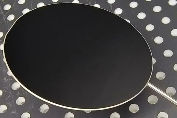
The first order of 1,000 pieces has not yet been delivered, and in less than a month, the customer placed another 1,000 pieces.
Since May 2023, the company has been receiving new orders since it realized the commercial production of 4-inch Gallium antimonide wafers.
QDHH has realized the mass production of 4-inch Gallium antimonide wafers, which marks a big step forward in the independence of China's Antimonide semiconductor material research and development and production.
Semiconductor core component – Gallium antimonide wafer

Gallium antimonide wafer substrate is a key material used to manufacture "Class II Superlattice infrared focal plane detector chip", which is the core component of infrared focal plane array detector.
Due to its ability to efficiently detect radiation within the infrared spectral range, the infrared detection distance can reach several kilometers away, and its sensitivity and resolution are extremely high, making it widely used in military, security, medical, and industrial fields.
According to SEMI data, semiconductor materials are the short board of the domestic Semiconductor industry chain, especially some products in wafer manufacturing materials are even more than 90% dependent on imports.
In previous years, due to less application, the research on Gallium antimonide in the field of semiconductor materials in China is far less in-depth than that on GaAs, Indium phosphide and other semiconductor materials.
However, with the release of market demand, in recent years, the Superlattice material Gallium antimonide has become a popular material in the field of infrared imaging, and the Antimonide semiconductor, as a classic Ⅲ – Ⅴ family system, also occupies the core position of the fourth generation semiconductor.
In 2019, some semiconductor materials, including Gallium antimonide, were restricted for export as Strategic material, which led to the serious impact on production of downstream enterprises that had previously relied heavily on imports due to the shortage of Gallium antimonide wafers.
"The indicators of Gallium antimonide are the top requirements in the industry, for example, the flatness should be less than 3 microns, but chips of other materials may be less than 15 microns."
Flatness is only one of the "harsh" requirements for Gallium antimonide wafers in the industry. The extremely strict dislocation density, high specifications of conductivity and uniformity, as well as the entire wafer being "scrapped with just one scratch" during the polishing and cleaning process… These requirements mean that the larger the wafer diameter, the harder it is to control defects, resulting in a decrease in yield and an increase in cost.
In February 2022, QDHH's first 2-inch Gallium antimonide single crystal successfully walked out of the crystal drawing furnace. On the basis of continuous technical iteration and improving the stability of yield rate, the team launched the research and development of 4-inch Gallium antimonide wafers with great effort. Only one year later, QDHH realized the stable supply of 4-inch Gallium antimonide for downstream enterprises.
It has the ability to produce 2 inch 120,000 pieces, 3 inch 60,000 pieces, and 4 inch 12,000 pieces of Gallium antimonide wafers annually, of which the domestic market share of 2 inch Gallium antimonide wafers is about 70%, and the yield rate is 95%, far higher than the industry level.
QDHH's R&D team also made breakthroughs in the R&D of 6-inch semi insulated GaAs wafers and 4-inch Indium arsenide wafers.
On the basis of continuing to optimize the production process of 4-inch Gallium antimonide wafers and improve the yield of products, the commercial production of 4-inch Indium arsenide and 6-inch semi insulating gallium arsenide wafers will be realized in 2024.
Product
2-4 inch Gallium antimonide GaSb wafer
Gallium arsenide GaAs wafer
Indium phosphide InP wafer
Indium antimonide InSb wafer
Customer reference
SMIC,Huawei,ZTE,Micron,Sk Hynix,UMC,Samsang,Intel,TSMC…


