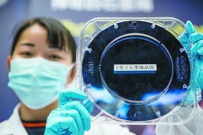
At the 2020 China International Graphene Innovation Conference held on October 16-18, new materials such as ultra-flat copper-nickel alloy single crystal wafers, 8-inch graphene single crystal wafers, and germanium-based graphene wafers were unveiled, showing China Innovative achievements in the field of high-quality graphene materials. Driven by the ZKSW graphene industrial technology functional platform, the scientific research team has realized the small batch production of these results, and the product size and quality are in the international "leading" position.

In 2009, the ZKSW research team aimed at the key problems in the preparation of graphene single crystals and the application of electronic devices, and began to tackle the key problems. "Just like the material used to make silicon chips is a piece of silicon single crystal wafer, if you want to use graphene and other carbon-based two-dimensional materials to realize the integration of electronic devices and start the revolution of microelectronics technology, you must prepare large-scale, high-quality graphene. Single crystal wafer." said Wu Tianru, associate researcher at ZKSW.
It can be described as "a sword in ten years". With the support of major national science and technology projects and scientific and technological innovation action plan projects, the ZKSW research team aims at the commanding heights of high-quality graphene preparation and high-performance device technology, and aims at the potential of wafer-level graphene single crystals. Control equipment, focusing on the development of new functions of graphene and the expansion of application areas. From growing a single layer to a single crystal, and then to an atomically flat large-area wafer, ZKSW finally allowed graphene to be peeled from a sample of a few microns with tape to an 8-inch wafer that can be mass-produced.
In order to achieve mass production of graphene wafers as soon as possible, ZKSW signed an agreement with the graphene functional platform in September last year to provide cost-competitive industrial applications. In addition, graphene materials with thin atomic layers can act as powerful sensors for various physical parameters (chemical composition, humidity, temperature, strain, etc.). These monolithic sensing platforms are used in conjunction with radio frequency identification antennas to be used as remotely readable detectors. .
The small batch production of graphene wafers has laid the foundation for the research and development of a new generation of electronic devices in China. Currently, some graphene-based electronic components for data communication are undergoing prototype demonstrations in the industry. Among them, electronic and photonic components have been integrated into the transmission system and have been verified to achieve high-speed, low-power data or telephone communication. The photoelectric module of the graphene photodetector can detect the entire wavelength range from visible light to heat. ZKSW subordinate units used newly developed materials to carry out research and breakthroughs in the core technology of electronic devices such as graphene terahertz detectors and high-performance radio frequency transistors.

