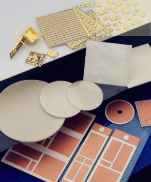
In 2018, China's leading electronic ceramic material technology group, HBZC Advanced Ceramic Technology Group, as the lead unit of China's electronic ceramics, has completed the national science and technology major project "Research and Industrialization of Aluminum Nitride Packaging Technology for IGBT". This project has broken through for IGBT packaging. The key material, aluminum nitride copper clad laminate preparation technology, has successfully realized commercial production.

Aluminum nitride ceramic substrate has the characteristics of high thermal conductivity, high electrical insulation, low dielectric, low thermal expansion, especially its thermal conductivity is about ten times that of alumina ceramic substrate, thermal expansion is equivalent to silicon chip, it is the most ideal toxic oxidation Beryllium substitute products.
About HBZC
HBZC is a high-tech enterprise specializing in the research and development, production and sales of electronic ceramic products. It is committed to becoming a world-class supplier of electronic ceramic products and providing customers with innovative, high-quality and competitive electronic ceramic products.
The company's main products include optical communication device housing, wireless power device housing, infrared detector housing, high-power laser housing, acoustic watch crystal housing, 3D optical sensor module housing, 5G communication terminal module housing, aluminum nitride ceramic substrate, ceramic components , Integrated heaters, etc., widely used in optical communications, wireless communications, industrial lasers, consumer electronics, automotive electronics and other fields. The company's electronic ceramic housing products are an important bridge for the connection of internal chips and external circuits in high-end semiconductor components, and have an important role and influence on the performance of semiconductor components.
The company's technical advantages are mainly reflected in the new electronic ceramic materials, semiconductor enclosure simulation design, and production technology.
In terms of advanced ceramic materials, the company independently masters three ceramic systems, including 90% alumina ceramics, 95% alumina ceramics and aluminum nitride ceramics, as well as their matching metallization systems.
In terms of design, the company has advanced design methods and design software platforms that can optimize the design of ceramic housing structure, wiring, electricity, heat, and reliability. The company has been able to design and develop 400G optical communication device housings, which is equivalent to the technical level of similar foreign products; it has the ability to simulate the thermodynamic reliability of ceramic materials such as alumina and aluminum nitride and new metal sealing, which can meet the heat dissipation and heat dissipation of the new generation of wireless power device housings. Reliability requirements; to achieve air-tight and high-strength structure design, the developed high-end fiber-coupled semiconductor laser package housing meets user requirements.

In terms of process technology, the company has a full set of multilayer ceramic shell manufacturing technologies, including raw material preparation, casting, punching and cavity punching, metal printing, lamination, hot cutting, sintering, nickel plating, brazing, gold plating and other technologies. The company has established a complete aluminum oxide ceramic and aluminum nitride ceramic processing technology platform. It has an aluminum oxide multilayer ceramic process based on tape casting, a high temperature thick film metallization process based on thick film printing, and a high temperature solder The main brazing assembly process and the nickel plating and gold plating processes mainly based on electroplating and electroless plating.

