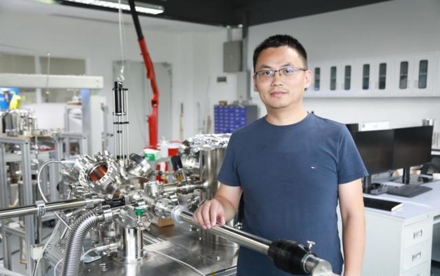
Through voltage control, nanometer-level precision displacement can be achieved, and it can be used in fields such as scientific experiments, precision manufacturing and semiconductor industry that require ultra-high precision. A few days ago, in the laboratory of the high-end scientific research equipment industrialization team of the Songshan Lake Materials Laboratory, the team leader Xu Zhi demonstrated the team`s piezoelectric driven nano-stage with core technology.
With the further development of microelectronics, nanotechnology and artificial intelligence, precision positioning is not only widely used in laboratories, but also more and more industrial applications. Based on previous research, the team has developed a series of ultra-precision positioning products with independent intellectual property rights, filling the gap in domestic production.

"This is one of our main products. In the past, the conventional drive positioning was controlled by a motor, but we used a material called piezoelectric ceramics, which produced a small deformation after electricity, and used this micron-level small deformation to make the table happen. Displacement.” Xu Zhi said. On the one hand, the piezoelectric driven nano-stage developed by the team has a large displacement range, and on the other hand, the positioning accuracy can reach a few tenths of a nanometer, which is nearly 10,000 times different from the ordinary micron-level positioning accuracy.
The team mainly focuses on three aspects: material growth, material characterization and material testing. "Our material growth equipment and the quality of the grown materials are better than others. This is our core competitiveness and the result of many years of accumulation in the laboratory." Xu Zhi said, material characterization belongs to the category of observation, through scanning probe microscope Wait for equipment to show the atomic structure of the material surface. In addition, using the equipment developed by the team can also perform atomic-level measurements and study the performance characteristics of materials under different conditions.
At present, in the innovative model factory, the team is committed to promoting the transformation from laboratory prototypes to mature products, improving product stability, ease of use and quality consistency, and gradually bringing products to the market.
Successfully realized industrial transformation of 4 invention patents
In fact, technology often has a large spillover effect, and the technology obtained from the development of scientific research equipment also has unexpected functions in other fields. In the laboratory, he showed reporters a special probe, the tip is as thin as one atom. "This needle can'touch' the surface of the material like a hand, and use atoms to'touch' the atoms. The operation accuracy is very high. By detecting the weak current change between the needle and the sample, the contact state can be judged to find out The arrangement of atoms on the surface of the material."
Relying on the innovative model factory of the material laboratory, the team is rapidly advancing the industrial application of products. At present, the precision instrument team has 4 independent intellectual property patents, 1 patent under review, and 5 patents to be applied for. The start-up company incubated by the team in the laboratory has been established for more than a year, and the contract value that has been signed and will be signed is nearly 10 million yuan.
松山湖材料实验室

